This product is manufactured by
SFA Semicon


Manufacturer information
SFA Semicon
Assembly and Test, Bumping, Packaging semi conductor manufacturing, Assembly, Inspection, Toll processing, Image analysis transport manufacturing
Inquiry
How to order
Problem with product info?
Update request
Manufacturer
SFA Semicon
Product Type
Machine
Brand
-
SKU
35727
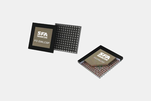
Product Name
FO-WLP : Fan Out Wafer Level Package
Model Name
-
Size
-
Weight
-
Product Details
More products

TO-220

QFP : Quad Flat Package

SD Card : Secure Digital Card

Micro SD Card : Micro Secure Digital Card

DIP : Dual In-line Package

SOP : Small Outline Package

TSOP : Thin Small Outline Package

QFN : Quad Flat No Leads

SIP : System in Package

PBGA : Plastic Ball Grid Array

FBGA Stack Die : Fine-pitch Ball Grid Array Stack Die

FBGA : Fine-pitch Ball Grid Array

FCCSP : Flip Chip Chip Scale Package

FCBGA : Flip Chip Ball Grid Array

CoC, CoW : Chip on Chip, Chip on Wafer
1/4