지금 보고 계신 제품의 제조사에요
HORIBA
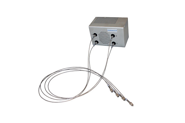
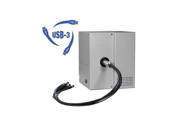
Miniature Spectrometers
모델명
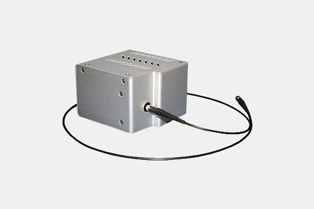
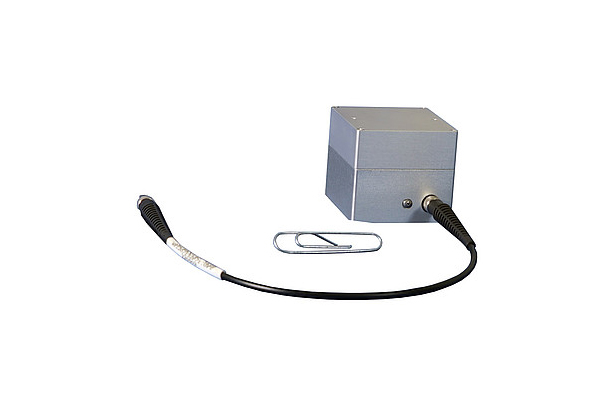
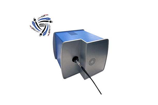
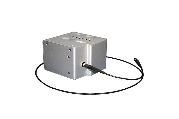
VS20-VIS
구매정보
HORIBA
정보 인증을 완료한 신뢰할 수 있는 기업입니다.
분광기, 분광 시스템, 그레이팅, 회절격자, 카메라 시스템, OEM 제조업체
연락처
+33 1 69 74 72 00
이메일
info-sci.fr@horiba.com
상품정보에 문제가 있나요?
정보수정 / 삭제요청
코머신은 제품 판매자가 아닙니다.법적고지 및 안내
제품 상세 정보
이 기업의 다른 제품
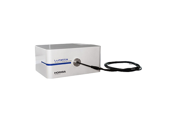
Multispectral Imaging SpectrometerLumetta
Hyperspectral Imaging SystemsPoliSpectra® H116
MultiTrack SpectrometerPoliSpectra® Quad
MultiTrack SpectrometerPoliSpectra® M116
UV-Vis-NIR SpectrometersInVizU Cube
UV-Vis-NIR SpectrometersVS70-MC
UV-Vis-NIR SpectrometersOES-Star
UV-Vis-NIR SpectrometersVS70-PDA
Gratings for astronomy
Laser Pulse Compression Gratings
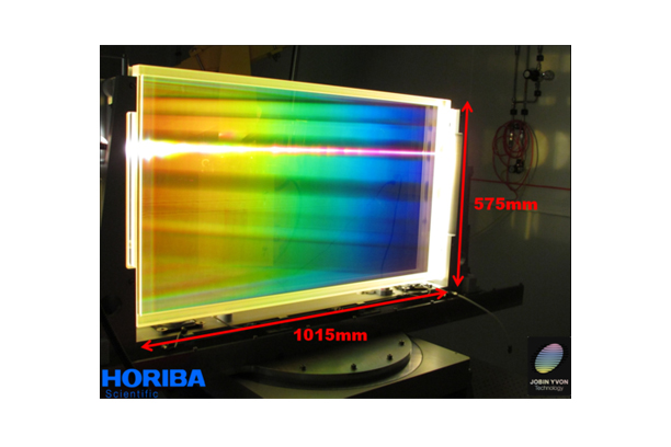
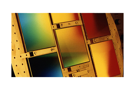
Holographic Concave Gratings - Type I
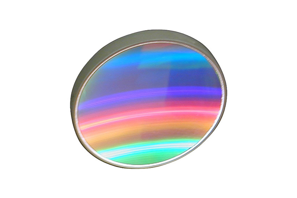
Ruled plane gratings
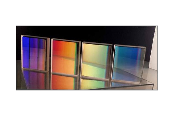
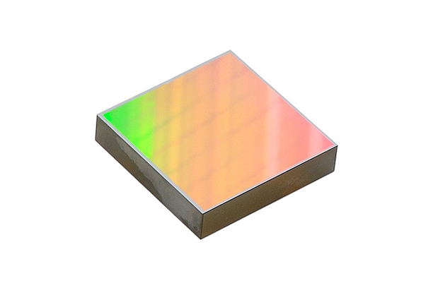
Blazed Holographic Plane Gratings
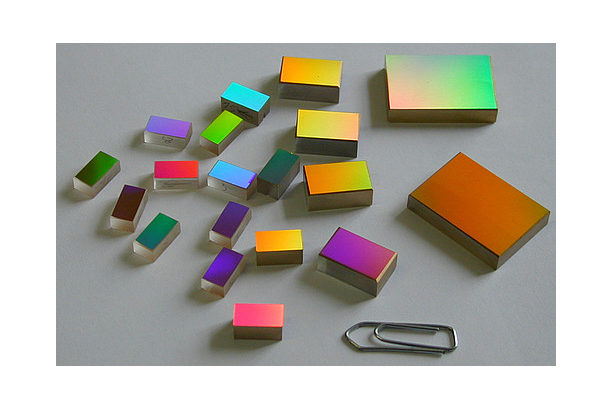
Holographic Plane Gratings
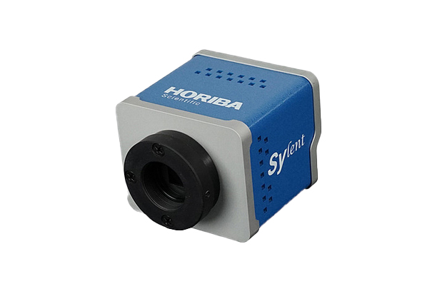
Scientific CMOS Imaging CameraSylent™
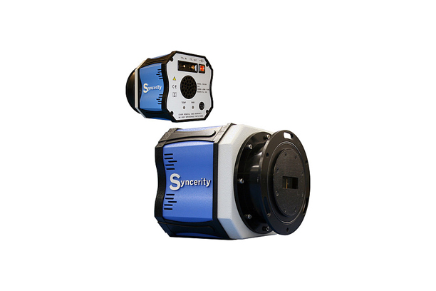
Syncerity Scientific CamerasFI-VU-VIS
1/4