


Information
209 Gyeongsu-daero, Uiwang-si, Gyeonggi-do, South Korea
+82 70-7507-1411
-
Overview
- Summary
- Saeron Technology is an electron beam specialist company that successfully localized the scanning electron microscope (SEM) for the first time in Korea in 2001. The company contributes to various industrial sectors such as nanomaterials, semiconductors, chemicals, and textiles, leveraging its proprietary electron beam optic design technology. It supplies a wide range of electron microscope products from low-end to high-end, along with electron beam welding equipment, earning recognition for its technological prowess in both domestic and international markets. The company focuses on providing customized products and differentiated application solutions tailored to customer needs.Saeron Technology is an electron beam specialist company that successfully localized the scanning electron microscope (SEM) for the first time in Korea in 2001. The company contributes to various industrial sectors such as nanomaterials, semiconductors, chemicals, and textiles, leveraging its proprietary electron beam optic design technology. It supplies a wide range of electron microscope products from low-end to high-end, along with electron beam welding equipment, earning recognition for its technological prowess in both domestic and international markets. The company focuses on providing customized products and differentiated application solutions tailored to customer needs.
- Key Products/Technologies
- Scanning Electron Microscopes (SEM) include various models such as Compact SEM, Normal SEM, PREMIUM LaB₆, FE-SEM, and Air SEM. The FE-SEM model, SEMIRON 5000, is a high-specification product launched in 2020, incorporating Schottky FEG technology. The AIS2500C is a LaB₆ SEM model launched in 2019, featuring a conical column for enhanced analytical capabilities. The AIS2300C, introduced in 2018, supports Digital Zoom 8X and Extreme Low KeV (≤ 1KeV) imaging. The Table Mini SEM AURA series, commercialized in 2014, represents a desktop mini SEM.Scanning Electron Microscopes (SEM) include various models such as Compact SEM, Normal SEM, PREMIUM LaB₆, FE-SEM, and Air SEM. The FE-SEM model, SEMIRON 5000, is a high-specification product launched in 2020, incorporating Schottky FEG technology. The AIS2500C is a LaB₆ SEM model launched in 2019, featuring a conical column for enhanced analytical capabilities. The AIS2300C, introduced in 2018, supports Digital Zoom 8X and Extreme Low KeV (≤ 1KeV) imaging. The Table Mini SEM AURA series, commercialized in 2014, represents a desktop mini SEM.
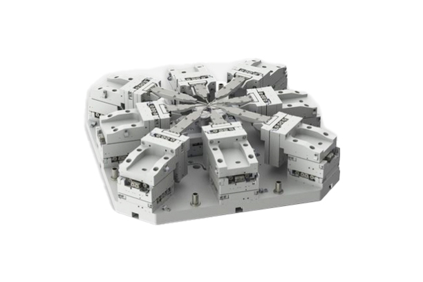
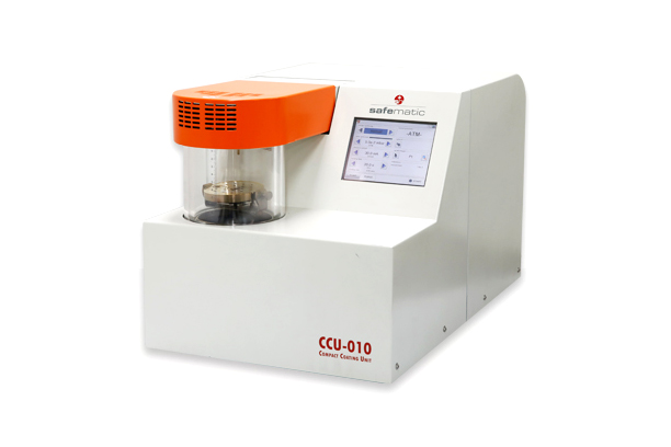
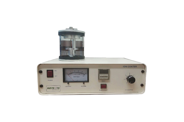
- Electron beam welding equipment includes E-Beam Micro Joining and E-Beam Welder (EBW) offerings. The company demonstrated its technological capability by developing the world's first Micro E-Beam Joining System in 2005. The Ion Sputter Coater is an essential piece of equipment for sample pre-treatment processes. Proprietary electron beam Optic design technology serves as a core competence for developing top-tier electron microscope products in Korea.Electron beam welding equipment includes E-Beam Micro Joining and E-Beam Welder (EBW) offerings. The company demonstrated its technological capability by developing the world's first Micro E-Beam Joining System in 2005. The Ion Sputter Coater is an essential piece of equipment for sample pre-treatment processes. Proprietary electron beam Optic design technology serves as a core competence for developing top-tier electron microscope products in Korea.
- The FE-SEM, SEMIRON, is equipped with auto-stepping and tiling functions for its motor stage, a powerful control drive system, and an innovative intelligent GUI. It achieves a high resolution of 1.0nm, optimizing it for observing and analyzing ultra-fine samples. The AIS2500C offers 2nm resolution and benefits from a conical lens for large-area sample observation.The FE-SEM, SEMIRON, is equipped with auto-stepping and tiling functions for its motor stage, a powerful control drive system, and an innovative intelligent GUI. It achieves a high resolution of 1.0nm, optimizing it for observing and analyzing ultra-fine samples. The AIS2500C offers 2nm resolution and benefits from a conical lens for large-area sample observation.
- Core Advantages
- Pioneering the domestic electron beam technology sector through the successful localization of scanning electron microscopes (SEM) for the first time in South Korea. This achievement stems from extensive research and development efforts initiated in 2001.Pioneering the domestic electron beam technology sector through the successful localization of scanning electron microscopes (SEM) for the first time in South Korea. This achievement stems from extensive research and development efforts initiated in 2001.
- Possession of proprietary electron beam Optic design technology, enabling the provision of Korea's highest-specification electron microscope products and customized solutions. This technological prowess is recognized internationally, earning the company a reputation as a 'Hidden Company'.Possession of proprietary electron beam Optic design technology, enabling the provision of Korea's highest-specification electron microscope products and customized solutions. This technological prowess is recognized internationally, earning the company a reputation as a 'Hidden Company'.
- A broad product spectrum, ranging from low-end to high-end models across all product categories, addressing diverse customer demands in both domestic and international markets. This strategy aims to secure both price competitiveness and advanced technological capabilities.A broad product spectrum, ranging from low-end to high-end models across all product categories, addressing diverse customer demands in both domestic and international markets. This strategy aims to secure both price competitiveness and advanced technological capabilities.
- Successful development of the world's fifth Field Emission Scanning Electron Microscope (FE-SEM), bridging a 35-year technology gap with a single leap of innovative technology. This contributes to reducing the reliance on imports for advanced industries like semiconductors and displays in Korea.Successful development of the world's fifth Field Emission Scanning Electron Microscope (FE-SEM), bridging a 35-year technology gap with a single leap of innovative technology. This contributes to reducing the reliance on imports for advanced industries like semiconductors and displays in Korea.
- Strengthening technological competitiveness through continuous investment in R&D and the provision of differentiated patented technologies and analytical solutions. This reflects the company's commitment to contributing to national scientific and technological advancement.Strengthening technological competitiveness through continuous investment in R&D and the provision of differentiated patented technologies and analytical solutions. This reflects the company's commitment to contributing to national scientific and technological advancement.
- Target Industries
- Microstructure analysis and research and development in the nanomaterials industry.Microstructure analysis and research and development in the nanomaterials industry.
- Process analysis, quality control, and ultra-fine sample observation and measurement in the semiconductor and display industries.Process analysis, quality control, and ultra-fine sample observation and measurement in the semiconductor and display industries.
- Material property analysis and new material development in the chemical and textile industries.Material property analysis and new material development in the chemical and textile industries.
- Supply of research and development equipment to leading domestic universities and national research institutes.Supply of research and development equipment to leading domestic universities and national research institutes.
- Major Markets
- China, India, Southeast AsiaChina, India, Southeast Asia
- Certifications/Patents
- On November 25, 2025, the AIS2500C-EL (E-Beam Litho.) model was designated as an Excellent R&D Innovation Product by the Ministry of Trade, Industry and Energy.On November 25, 2025, the AIS2500C-EL (E-Beam Litho.) model was designated as an Excellent R&D Innovation Product by the Ministry of Trade, Industry and Energy.
- In 2021, the CEO received a commendation from the Minister of Science and ICT, marking the third such award after those from the Ministry of Trade, Industry and Energy and the Small and Medium Business Administration.In 2021, the CEO received a commendation from the Minister of Science and ICT, marking the third such award after those from the Ministry of Trade, Industry and Energy and the Small and Medium Business Administration.
- In 2016, the company received the Product Innovation Award at the Korean Electronics Show (KES), the Nanotechnology Day Achievement Award (Minister of Trade, Industry and Energy commendation), and a commendation from the Nano Korea Organizing Committee (Industrial Technology sector).In 2016, the company received the Product Innovation Award at the Korean Electronics Show (KES), the Nanotechnology Day Achievement Award (Minister of Trade, Industry and Energy commendation), and a commendation from the Nano Korea Organizing Committee (Industrial Technology sector).
- New Technology (NET) certification acquired in 2016.New Technology (NET) certification acquired in 2016.
- Innobiz certification and Technology Innovation Award (Nano Korea Organizing Committee) received in 2010.Innobiz certification and Technology Innovation Award (Nano Korea Organizing Committee) received in 2010.
- Possession of 5 patent applications and 4 registered patents related to FE-SEM digital driving drivers.Possession of 5 patent applications and 4 registered patents related to FE-SEM digital driving drivers.
Introduction
Key Products


Location
209 Gyeongsu-daero, Uiwang-si, Gyeonggi-do, South Korea
클릭하여 위치 살펴보기
